The Quiet Photonics Revolution
AI's Heat Wall - and Emerging Investment Opportunities on the Horizon

Two years into the generative AI supercycle. The models are smarter than ever - some would argue amazing, even. Yay! …maybe
…I’ll set existential concerns aside for the moment…
AI’s inferrential potential is not just software-driven or model-constrained. It fundamentally relies on hardware throughput. That througput is constrained by the limitations of electron-based computational systems. Those systems are hitting an insurrmountable heat wall. Copper traces on silicon chips are becoming resistive highways, choking bandwidth and generate unscalable and unsustainable amounts of heat.
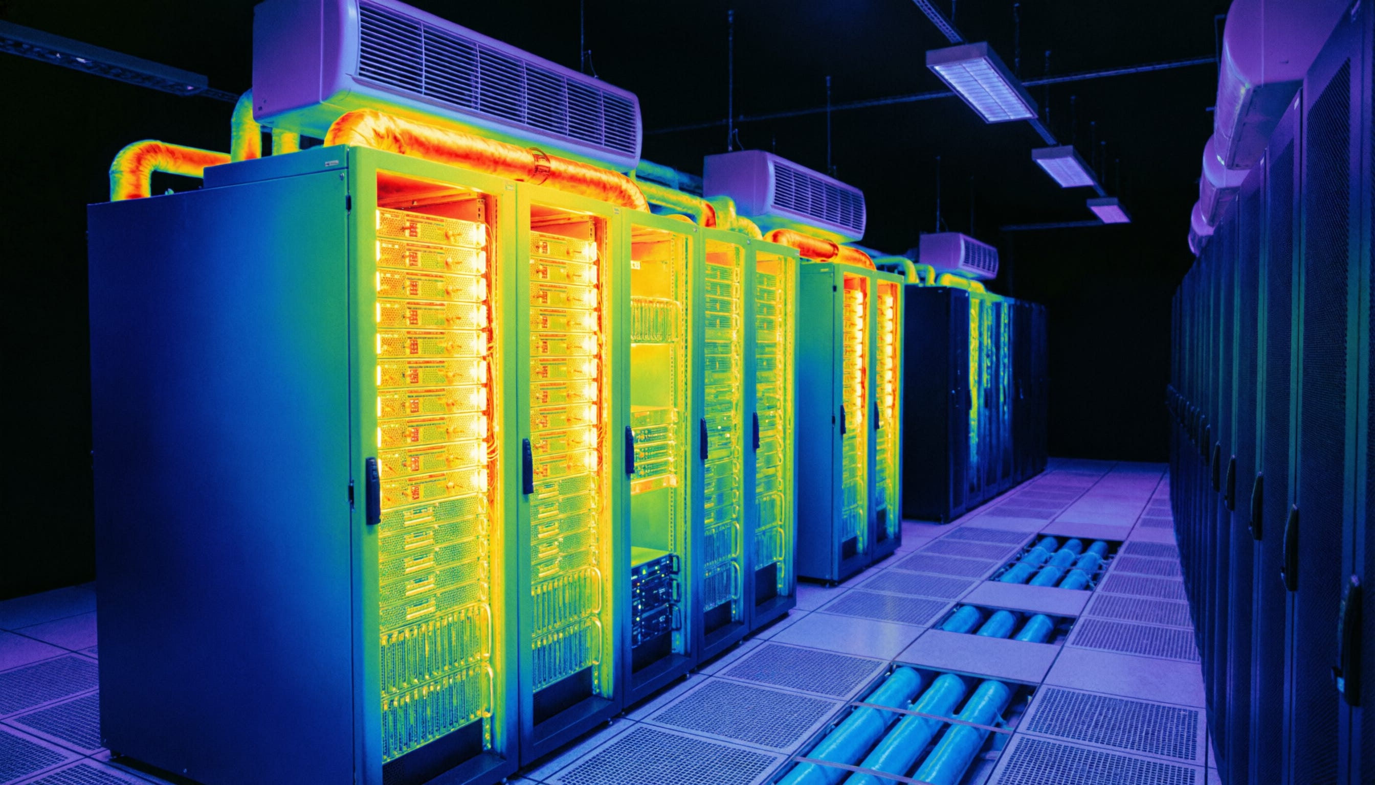
The AI buildout, is shifting from “How many GPUs can we buy?” To “How do we move data without melting the planet.
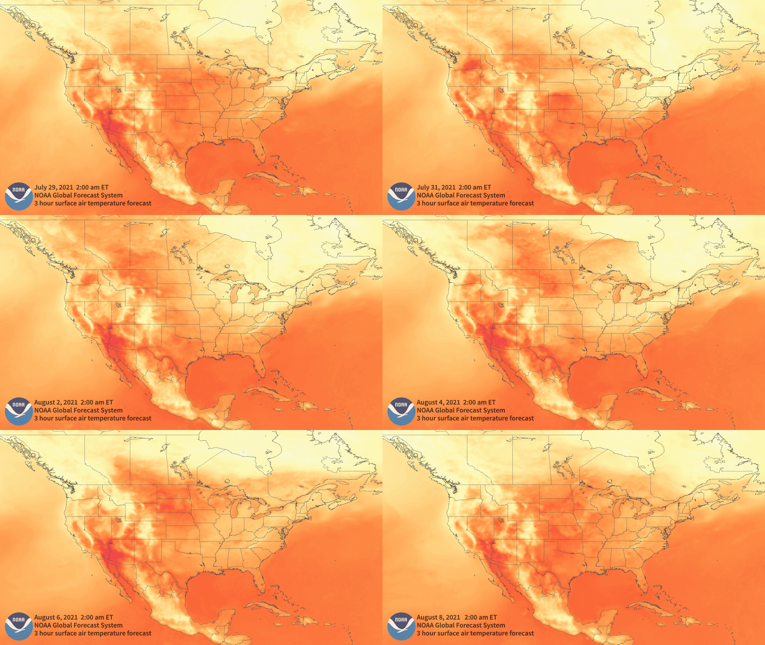
The answer lies not in better silicon chips, but in leaving silicon behind. The future of compute is becoming photonic ...one step at a time.
Let’s explore how this shift will define the next decade in terms of CAPEX investments and which companies are at the tip of the spear, building components for systems urgently in demand today.
The Four Chokepoints of Modern Compute
The current AI hardware stack—dominated by semiconductor chips and transistors moving electrons through copper—are facing four distinct walls.
The Energy Wall: Training a frontier model in 2026 costs millions in electricity alone. Inference is worse. As we move from training to ubiquitous inference, the power density required per rack exceeds what the grid can reliably supply in key regions. Electrons generate heat via resistance; the more you push them, the more energy you waste as thermal noise.
The Memory Wall: Processors are starving. Compute speed has outpaced memory bandwidth. Moving data from HBM (High Bandwidth Memory) to the logic unit consumes more energy than the actual calculation. This is the “von Neumann bottleneck,” and it is strangling efficiency.
The Interconnect Wall: Clusters are growing larger. Moving data between GPUs across a rack requires serdes (serializer/deserializer) that struggle beyond 224 Gbps per lane without significant signal loss. Copper traces on a motherboard are becoming too lossy at high frequencies.
The Latency Wall: For real-time AI (robotics, high-frequency trading, autonomous systems), the microseconds lost in electrical conversion and routing are unacceptable.
The Photonic Solution (and some new friction)
Photonics replaces electrons with photons. Light generates no heat when moving through a waveguide, offers vastly higher bandwidth density, and is immune to electromagnetic interference.
How it alleviates chokepoints:
Optical Interconnects: By moving data via light between chips (chip-to-chip) or within packages (co-packaged optics), we bypass copper resistance. This slashes the energy per bit transmitted by up to 10x. (Key Players: Cisco Systems, Arista Networks)
Optical I/O: Instead of converting optical signals to electrical ones at the server rack edge, we bring optics directly to the processor die. This removes the power-hungry electro-optical converters from the critical path. (Key Players: Intel Corporation [Silicon Photonics], GlobalFoundries)
Analog Optical Compute: For specific AI workloads (matrix multiplications), light can perform calculations physically as it passes through interferometers, theoretically offering near-zero latency and ultra-low energy consumption for inference. (Key Players: Lightmatter, Luminous Computing [Private])
The New Chokepoints:
However, photonics is not a magic wand. As we integrate light into the compute stack, new friction points emerge:
The Coupling Loss: Getting light from a fiber (microns wide) into a silicon waveguide (nanometers wide) is incredibly difficult. Misalignment by a fraction of a micron kills the signal. This drives up packaging costs and lowers yields. (Solutions providers: ASMPT, Coherent Corp.)
The Laser Thermal Issue: While light doesn’t generate heat when moving, generating light does. Integrating lasers directly onto CMOS chips (hybrid integration) creates localized hot spots that require novel cooling solutions. (Solutions providers: II-VI Incorporated [now Coherent], IPG Photonics)
Signal Integrity & Error Correction: Optical signals degrade over distance and can be noisy. We are shifting from managing electrical resistance to managing optical signal-to-noise ratios, requiring new error correction codes that add computational overhead. (Solutions providers: Synopsys, Cadence Design Systems)
Integration: A Near-term Hybrid Reality
In the present-day buildout (2026-2028), we see the rise of Co-Packaged Optics (CPO). Instead of pluggable optical transceivers on the edge of a switch, the optical engine is packaged alongside the ASIC or GPU. This is already being deployed in high-end networking switches to support the clustering required for trillion-parameter models.
For training models, the architecture remains largely electronic (CUDA cores), but the communication fabric becomes optical. For inference, however, we will see specialized optical accelerators offloading specific matrix operations. This allows existing software stacks (PyTorch, TensorFlow) to remain largely intact while the hardware underneath swaps copper for glass.
A Decade of Light: 2026-2036 Timeline
Based on current research trajectories and pilot programs visible today, here is the projected roadmap for alleviating these bottlenecks:
2026-2028 (The Interconnect Layer): Widespread adoption of Co-Packaged Optics in data center networking. Electrical I/O remains on the chip, but off-chip communication goes optical. Marvell Technology currently leads in DSPs to allieviate the this. But there are LOTs of gems to find here.
2029-2031 (The IO Layer): Introduction of Optical I/O standards (like UCIe but optical). Memory and processors communicate via light buses. This drastically reduces the energy cost of moving data from memory to compute. Rambus, Astera Labs making signal processors that bridge chips to ‘talk’ to light.
2032-2034 (The Compute Layer): Commercial deployment of specialized photonic inference engines for high-volume, low-latency tasks (e.g., edge AI, autonomous vehicle processing). Alleviates: Energy & Latency Walls. Broadcom is a leader here, producing high-speed minimal-latency serial/deserial optical DSPs. But this area will evolve. … a lot.
2035+ (The Quantum/Analog Hybrids): Photonic links become the standard backbone for connecting quantum processors to classical supercomputers, enabling hybrid algorithms that leverage quantum speedup for specific optimization tasks within AI training. Alleviates: Capacity Wall. IBM, IonQ, PsiQuantum will probably be active in the longer-term of optics and quantum processing.
Investment Implications
We are standing at an inflection point similar to vacuum tubes —> transistors. This time it’s electrons —> photons. Tracking key players solving the packaging yield problem and the laser integration problem are critical to building a future-proof investing portfolio with a focus to present and future hardware buildouts.
The CAPEX required to retool fabrication lines for photonic integration is massive. This creates a high moat for incumbents but also presents massive opportunities for specialized suppliers who can bridge the gap between silicon foundries and optical component manufacturers.
Stay Tuned
Next we shall some companies who are best positioned to profit from this photonic pivot. We will examine who owns the IP on low-loss coupling, who is dominating the CPO supply chain, and which “picks and shovels” players are flying under the radar.
Stay Curious
This is awesome Diggi! Thanks for writing on such an interesting topic